- Deutsch (de)
- English (en)
 Everyone knows the problem that circuits or wiring do not work due to short circuits or interruptions. The domestic multimeter offers a continuity tester that acoustically reveals a low-resistance connection. It only becomes difficult if the location of the short circuit does not reveal itself immediately. A tonohmmeter can be used for such cases. This means that the measured resistance is mapped to the associated pitch. The smaller the resistance, the higher the tone. If the measuring range is sensitive enough, you can get closer to the cause.
The device from my student days has unfortunately reached the sacred silicon sky and is no longer with me. So why not build a new microprocessor-controlled device based on an AVR.
The device has to meet the following requirements:
 The resistance is measured via the voltage drop. In order to be able to carry out measurements within circuits, a square-wave signal with approx. 340mV (the usual ESD structures of the ICs do not open) is released onto the unknown resistor. The resulting voltage drop is then amplified and rectified via OpAmps. The AVR does the AD conversion and audio output.
The center of the power supply is a LiPo with a nominal 3.7V. It is charged with a maximum of 4.2V and 500mA. A MAX1811 (IC5) takes over the entire charge control. The AVR is supplied with a stable 3.0V via a controller (IC1). The Charge Pump C6 / D1 also comes with the negative voltage (-2V) required for the OpAms. The analog part can be switched off in the idle state via Q1. The charge level is estimated by the voltage value on the LiPo (R25 / R26).
Due to the design, it can lead to deep discharge and thus to destruction of the LiPo. The AVR detects the undervoltage and does not start, but the LiPo is further discharged by the quiescent current. The only remedy is an additional battery management system (PCB protection circuit), which is available from LiPo suppliers for little money (e.g. PCB 2.5 A 1 cell Lipo Li-ION -259). Due to the small design (15.0 x 4.0 x 2.5 mm) the PCB fits into the housing later. So nothing can happen to the LiPo anymore.
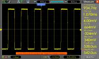
The AVR generates the square wave signal of approx. 1KHz on PA6. The level conversion is carried out by IC3A and the Schottky diodes (D2) limit the voltage swing. Since we want to get close to Milliohm, the measuring line has to be compensated. Therefore, the connection of the measuring terminals is made via 2.5mm jack sockets to which the two-pole measuring cable is first connected. This is followed by a two-stage amplification circuit with a low pass. The gain of the second stage can be controlled via a programmable resistor (IC4). The AVR can determine the resistance value and thus the gain via a bidirectional SPI. The signal amplified in this way is rectified by IC3D and fed to the AVR for the purpose of AD conversion.
The device is only operated via one key (U1). The hardware debouncing (C8 / R3 / R4) avoids the otherwise necessary software. The measuring range is displayed via three LEDs (LED2-4) and the sound output is performed by a small loudspeaker that is capacitively connected to the digital port. That is enough for simple tones. After all, we don't want to output MP3.
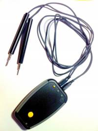
Since I liked the handheld housing from HAMMOND, it was difficult to find a LiPo that was the right size. Unfortunately I only found one for the front, so the board got a bit tight and is populated on both sides. At one end are the two jack sockets for the measuring strips and at the bottom the charging socket with charge indicator. The unused routing area is designed as a ground area. The AVD-ISP connection can be seen on the left, which enables us to do on-board programming.
The program needs less than 2K which is why an ATTINY24 would be sufficient. Because of that - you never know - I took the ATTINY44 anyway. The program development as usual in C on AVR Studio6 and debugged with AVR-DRAGON.
The SPI interface to the programmable resistor (POT) has done a little work. On the one hand, the POT requires a bidirectional data pin (SDI and SDO together) and, on the other hand, I could not abuse the USI because it was on unfavorable ports. The S/W emulation then looks like this:
// SPI write emulation (with SDI/SDO multiplexing)
void SPI_write(uint8_t addr, uint16_t data)  {
	TIMSK0 &= ~(1<<OCIE0B); 		// Stop 1KHz (PA6)
	TCCR1B = 0;					// stop timer (no tone signal)

	PORTA |= (1<<PA6) | (1<<PA4);	// SCK=SDIO HIGH
	DDRA |= (1<<PA6) | (1<<PA4);	// SCK+SDIO to output

	PORTA &= ~(1<<PA2);			// CS low

	// Address AD0..3 (bit15...12)
	for (i=3;i>=0;i--) {
		PORTA ^= (1<<PA6);		// SCK = LOW
		if ((addr & (1<<i)) == 0)
		PORTA &= ~(1<<PA4);
		else
		PORTA |= (1<<PA4);
		PORTA ^= (1<<PA6);		// SCK = HIGH
	}

	// Command C1,C0 (bit11,10)
	PORTA ^= (1<<PA6);			// SCK = LOW
	PORTA &= ~(1<<PA4);			// Data = LOW
	_delay_us(5);
	PORTA ^= (1<<PA6);			// SCK = HIGH
	_delay_us(5);
	PORTA ^= (1<<PA6);			// SCK = LOW
	_delay_us(5);
	PORTA ^= (1<<PA6);			// SCK = HIGH

	// Data D9..0 (bit9..0)
	DDRA |= (1<<PA4);				// set SDIO to output
	for (i=9;i>=0;i--) {
		PORTA ^= (1<<PA6);		// SCK = LOW
		if ((data & (1<<i)) != 0) {
			PORTA |= (1<<PA4);
		} else {
			PORTA &= ~(1<<PA4);
		}
		PORTA ^= (1<<PA6);		// SCK = HIGH
	}

	PORTA |= (1<<PA2);			// CS to HIGH
	DDRA |= (1<<PA4);				// SDIO to output

	TIMSK0 |= (1<<OCIE0B);			// Restart 1KHz (PA6)
	TCCR1B |= (1<<WGM12) | (1<<CS11);	// Restart TIMER with CLK/8
}
The complete program can be found in the download area below.
The device is switched on by pressing the button. For the first two seconds, the charge status of the battery is shown by the three yellow LEDs (3 LEDs at> 75%, 2 LEDs> 50% and one above 25%). If the battery capacity is below 25%, it must first be recharged. The circuit remains in sleep mode. After a successful start, an acknowledgment tone sounds for 2 seconds and the device is ready for use. The measured resistance value is converted into a suitable frequency from 500Hz to 2 KHz - provided it is in the measuring range - output. The measuring range is changed by pressing the button again. If you keep the button pressed for more than 2 seconds, the device switches to sleep mode and switches off.
Although mainly SMD components are used due to the lack of space, the board can be easily soldered. I soldered the back with the SMD components using the pizza pan method of the c't hacks. The front with the controls then hold by hand. In order to fit into the housing, the 2×3 post connector must be shortened by hand. A bit of drilling and filing is required for the case. A drilling template is available in the download area to help you.
True to the motto: a finished software is outdated, the current S / W version has the basic functions described but can always be improved. Incidentally, the power requirement in operation without sound output is approximately 13 mA, with sound output 23 mA. Stand-by hits with 215uA. So you can get by for half a year without reloading. In continuous operation you probably get 2-3 days. The practical test at home will hopefully confirm this.
The circuit board can be obtained from me at cost price of EUR 7.00 (as long as the sample stock lasts).
If you like my articles feel to donate a cappuccino or so…